Responsible
Research Area
Research Lines
Activities
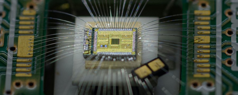
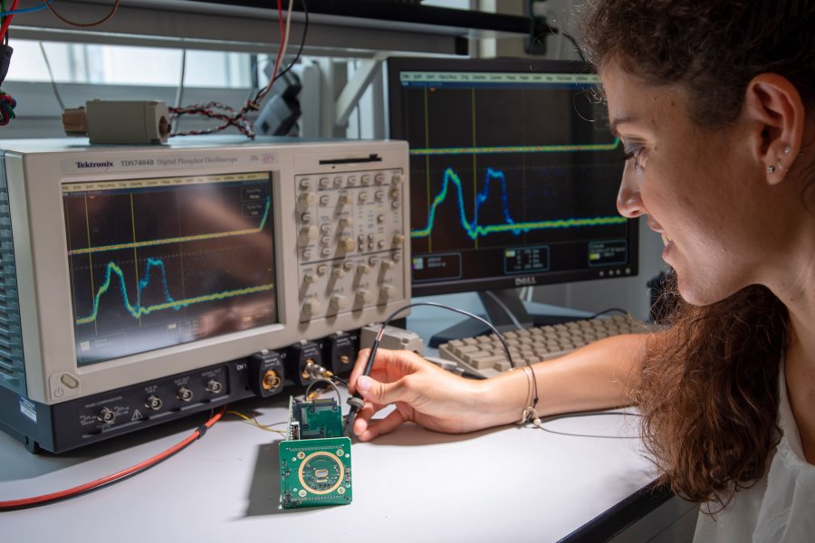
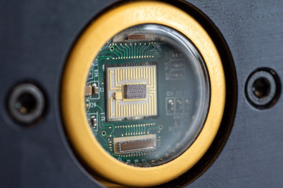
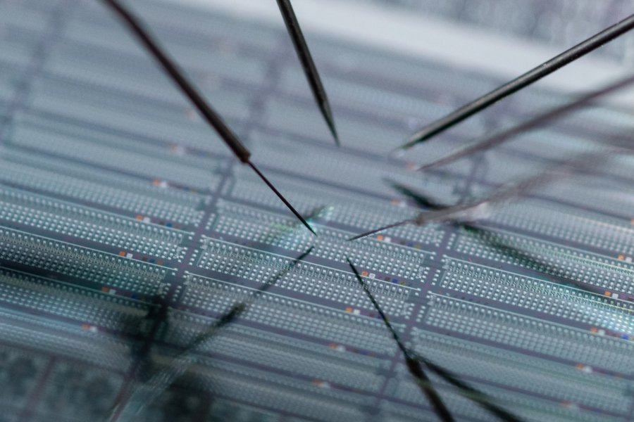
The lab research activities deal with the design, development and exploitation of microelectronic single-photon detectors, for the visible and near-infrared wavelength ranges, both as single pixels and as arrays for 2D imaging and 3D ranging acquisitions, and the associate electronic instrumentation for counting, timing and imaging single photons.
- Microelectronic Single Photon Avalanche Detectors (SPAD).
The lab is a pioneer in this field and presently is leader at an international level in the development of Single Photon Avalanche Diodes (SPADs) and the associate electronics. The lab introduced the “Active-Quenching Circuit” (AQC) concept, which opened the way to the practical application of this kind of detectors, and for the first time it developed monolithically integrated AQCs that became the enabling technology for the development of miniaturized analytical systems. The lab designed several generations of silicon SPADs (both single pixel and arrays) with innovative geometries and architectures, by means of technologies and processing developed through scientific collaborations, intensified in the last years, with the Microelectronics and Microsystems Institute of CNR for custom processing and other CMOS international foundries for VLSI processing. The exploitation of standard CMOS technologies for SPADs allowed the integration of SPAD detectors together with in-pixel analog electronics and digital processing inside the sensor chip, thus enabling the deployment of complex imaging systems with single-photon sensitivity and able to measure the photon time-of-flight with picosecond accuracy. In order to extend photon sensitivity to the infrared spectral range (beyond 1 micron), the lab developed single-photon detectors in Germanium and III-V semiconductors. An InGaAs/InP SPAD was conceived and developed together with high-performance electronics; thanks to the very fast GHz gating, the typical bottleneck (afterpulsing) of such detectors was definitely avoided, thus enabling counting rates beyond 100 Mcounts/s.
- SPAD applications.
The lab exploited SPAD devices and AQC electronics to different fields in collaboration with several research laboratories at an international level. Since several years, major applications are in the fields of micro- and nano-analytical systems (for DNA and protein analysis, molecular imaging, time-resolved near-infrared spectroscopy, etc.), 3D ranging (for automotive safety driving, monitoring of woods, security control of critical areas, etc.), quantum information (quantum cryptography, quantum computing, etc.), optical testing of VLSI integrated circuits.
Service information
The activity takes place in laboratories located in Building 24 of the electronics section of DEIB, in C. Golgi 40.


