Research Area:
Responsible:
Participants:
Research Lines:
Project abstract
The PULLNANO project was sponsored by the European Commission within the 6th Framework Program and it was focused on advanced Research and Technological Development activities to push forward the limits of CMOS technologies. It aimed at the development of 32 and 22nm CMOS technology nodes, opening the way to the long term future of these technologies. The project was a collective effort of 38 European partner organizations, including leading chip manufacturers, industry-orientated research institutions, universities and SMEs (Small and Medium Enterprises).
PULLNANO was a reference project and a unique opportunity to increase the worldwide impact of European Nanoelectronics and to create the conditions for future IST application.
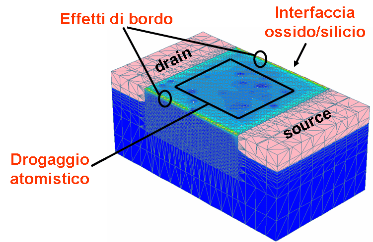
The project started on June 2006 and ended in November 2008. DEI's group contributed to efforts on advanced modeling and simulations. The target was on the development of advanced physical models addressing the needs foreseen for the 22nm technology node.
The following options were considered: strained silicon, different crystal orientations for the channel, high-k gate dielectrics as well as the impact of fluctuations of dopants, dielectric and silicon layer thickness and effects of line-edge roughness. The models were implemented in device simulators, comparing different device architectures and technological options.
Project results
- Development of new methods for dielectric reliability analysis and electromigration of interconnects for 32nm node structures.
- Design rules for feasible air gaps packaging and CMP testing on SD air gap structures and porous dielectric structures for 32nm node.
- Characterization of the microstructure and the electrical properties of Cu lines in 32nm node geometry.
- Ageing and reliability procedure of interconnections.
- Experimental packaging feasibility on multilevel air gaps (emphasis on wire bonding).
- Technical reviews publications.