Activities
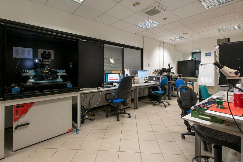
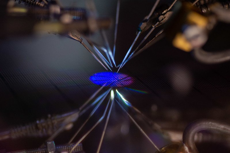
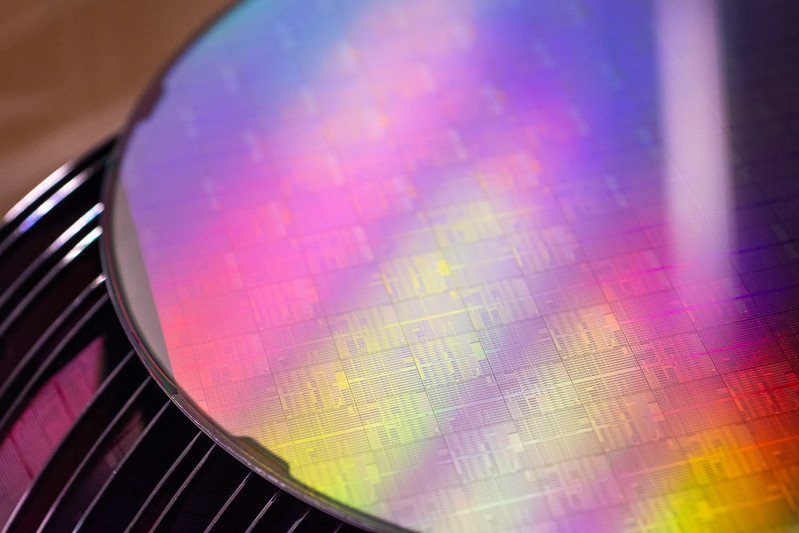
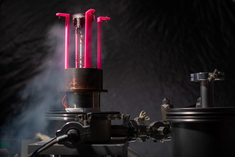
Solid-state memories have been playing an increasingly important role in the world of electronics, thanks not only to the large variety of applications currently arising from the unprecedented bit storage density of nanoscale technologies but also to the prospects of new memory-enabled computing paradigms on the horizon. In this context, the research activities performed in the lab are mainly focused on the experimental and numerical investigation of the basic physics, the reliability and the performance of nano-electronic devices for high-density data storage and in-memory computing. 3D-NAND Flash, NOR Flash, Phase-Change Memories (PCM), Resistive Random Access Memories (ReRAM), Magnetoresistive Random Access Memories (MRAM) and Ferroelectric Memories are just the most relevant technologies investigated in the lab. All the experimental samples under test are either provided by top semiconductor manufacturers or fabricated at the PoliFab (the Politecnico’s facility for the fabrication of micro and nano devices and structures). Experimental activities are carried out by means of advanced equipment for semiconductor device testing, such as probe-stations for wafer-level electrical characterizations, semiconductor parameter analyzers, high-speed arbitrary waveform generators, precision LCR meters, high-speed oscilloscopes, a cryostat and many other instruments and tools which are essential in any well-equipped nano-electronic lab. Numerical activities are performed by means of a commercial simulator of semiconductor devices (Synopsys TCAD) or through in-house software developed with Matlab.
Among the major aims of the research, it is worth mentioning the understanding of the basic phenomenology, the main dependences and the impact on the technology of the variety of physical phenomena taking place in solid-state nano-electronic devices for high-density data storage, exploring also the possibility to exploit these devices for the emerging in-memory computing scenarios.
The work is done in collaboration with some of the most important semiconductor companies in the world, among which it is worth mentioning Micron Technology Inc. and STMicroelectronics, or under the framework of national and international research projects.
Service information
The Lab is at the fourth floor of Bld. 22 (Via Golgi no 42, Milan)


