IEEE Photonics Society Distinguished Lecturer
DEIB - Alpha Room (building 24)
January 17th, 2018
9.30 am
Contacts:
Alberto Tosi
Research Line:
Single-photon detectors and applications
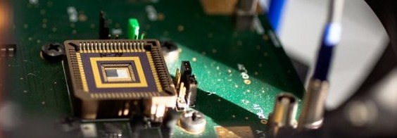
CMOS SPADs have appeared in 2003 and soon have risen to the status of image sensors with the creation of deep-submicron SPAD technology. The format of these image sensors has expanded from 8x4 pixels of our first LIDAR in 2004 to 512x512 pixels of recent time-resolved cameras, and the applications have literally exploded in the last three years, with the introduction of proximity sensing and portable telemeters. The current promise is that SPAD based sensors will be in every smartphone by 2018 and in every car by 2022. But SPAD technology was born for scientific applications and in scientific applications it will continue to innovate. For instance, super-resolution microscopy has already benefitted from SPAD imagers and this trend is expected to continue well in the next decade. In addition, other time-resolved techniques, such as time-of-flight PET, NIROT, FLIM, FRET, useful in many biomedical imaging modalities, will become more and more accurate and less and less expensive thanks to the scalability of CMOS technologies. With the introduction of SPADs in 3D CMOS IC technologies in 2014, SPAD based imagers will be more compact, while at the same time more advanced techniques and functionalities will be available. In the talk I will give a technical and economic perspective on SPADs and SPAD imagers, and a vision for the medium to long term.
Edoardo Charbon (SM’00 F’17) received the Diploma from ETH Zurich, the M.S. from the University of California at San Diego, and the Ph.D. from the University of California at Berkeley in 1988, 1991, and 1995, respectively, all in electrical engineering and EECS. He has consulted with numerous organizations, including Bosch, X-Fabs, Texas Instruments, Maxim, Sony, Agilent, and the Carlyle Group. He was with Cadence Design Systems from 1995 to 2000, where he was the Architect of the company's initiative on information hiding for intellectual property protection. In 2000, he joined Canesta Inc., as the Chief Architect, where he led the development of wireless 3-D CMOS image sensors. Since 2002 he has been a member of the faculty of EPFL, where is a full professor since 2015. From 2008 to 2016 he was with Delft University of Technology’s as Chair of VLSI design. He has been the driving force behind the creation of deep-submicron CMOS SPAD technology, which is mass-produced since 2015 and is present in telemeters, proximity sensors, and medical diagnostics tools. His interests span from 3-D vision, FLIM, FCS, NIROT to super-resolution microscopy, time-resolved Raman spectroscopy, and cryo-CMOS circuits and systems for quantum computing. He has authored or co-authored over 250 papers and two books, and he holds 20 patents. Dr. Charbon is a distinguished visiting scholar of the W. M. Keck Institute for Space at Caltech, a fellow of the Kavli Institute of Nanoscience Delft, and a fellow of the IEEE.